The Phototransistor
Mullard Ltd Reference Manual of Transistor Circuits, 1960.
Front cover
The phototransistor is a junction transistor, manufactured in such a way that the inherent photoelectric properties are fully exploited. It is essentially a photodiode, in which the light current is amplified by normal transistor action.
Photodiode
The mobile current carriers on the two sides of an isolated p-n junction will diffuse across the junction, until a counter-emf is built up which limits the further exchange of carriers. When a reverse voltage is applied to the diode, the barrier potential is increased correspondingly until equilibrium is again reached. Under these conditions, some carriers receive sufficient random energy to cross the barrier, and constitute the normal leakage current. This is the dark current.
If light is allowed to fall on the junction, hole-electron pairs are created on both sides of the junction. The barrier potential sweeps the holes one way and the electrons the other. The current now flowing is the light current, equal to the dark current plus the photoelectric current.
Phototransistor
The phototransistor operates like a normal transistor into which light is allowed to enter. The hole-electron pairs generated by the incident light should preferably be created as near to the collector junction as possible, in order to minimise recombination. Hole-electron pairs stand very little chance of contributing to the light current, if they are generated more than one diffusion length (usually about 0.5mm) from the collector junction.
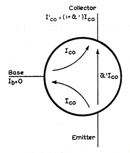
FIG. 1. Relation of I′co to Ico.
With the base open-circuit (Fig. 1), the leakage current Ico, which is only a few micro-amps, is transformed by transistor action into I′co, which is equal to (1 + α′)Ico. The dark current with the base open circuit is substantially equal to I′co.
When light falls on the phototransistor, the photoelectric current Iph contributes an internal base current which, if the base is open circuit, is amplified by the factor (1 + α′) into a much larger current at the collector. The light current in this circuit is approximately (1 + α′)Iph + I′co = (1 + α′) (Iph + Ico). Provided the photoelectric current is large in comparison With Ico, the light- to dark-current ratio is high.
Normally, the phototransistor is operated with a resistance between base and emitter, to ensure thermal stability at higher temperatures. The dark current (I′co) is then reduced considerably below its value with open-circuit base, resulting in a greatly improved light- to dark- current ratio.
OCP71 Phototransistor
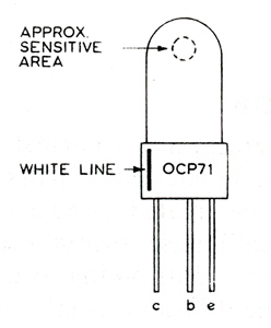
FIG. 2. Base connections of OCP71
The OCP71, which operates on the principles just described, is a general-purpose device of pnp alloy-junction construction. The base connections are as shown in Fig. 2.
Sensitivity and Response
Maximum spectral response occurs at a wavelength of 1.55μ, and 50% response is obtained at about 0.8μ and 1.6μ. (The micron μ is 10-6 of a metre, and is equal to 10,000Å.) The peak response is in the near infra-red, but continues through the visible spectrum to the near ultra-violet.
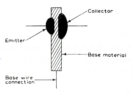
FIG. 3. Diagrammatic cross-section of OCP71.
Light falling on the emitter side of the crystal creates hole-electron pairs in the parts of the base not in the shadow of the emitter (Fig. 3). The chief contribution to the total light current is made by hole-electron pairs which have only a short distance to diffuse before reaching one of the junctions. The emitter junction of the OCP71 is smaller than the collector junction. The hole-electron pairs generated in an annulus (doughnut), the inner and outer boundaries of which are formed by the emitter and collector, are therefore most effective.
If the light is incident on the collector side of the crystal, the collector shades the annulus bounded by the emitter and collector. Hence fewer hole-electron pairs are created, and recombination is greater, and the total light current is very much smaller. However, the moisture-proof grease in which the assembly is coated diffuses the light, and the device is not critically sensitive to its direction.
Maximum current is obtained when the light is allowed to fall on the side of the bulb bearing the type number (Fig. 2), in a direction perpendicular to the plane of the leads. The response is about 50% of the maximum, when the light is incident at 90 degrees to this direction in the horizontal plane. If the light falls vertically downwards, the response is still 30%, of the maximum.
Output Current
The output (Ic/Vc) characteristic of the OCP7l is plotted for a number of intensities of incident light. The intensity, which is specified in foot-candles ( = lumens/ft2), has to be calculated in order to interpret this characteristic.
The amount of light (in lumens) falling on any surface is given by
(Candlepower of source x Area of surface) / ( (Distance of surface from source)2
For example, if a 40W tungsten-filament electric lamp (which gives approximately 30 candlepower) is placed 120mm from a surface 7mm2 in area, the flux at the surface is
(30 x 7) / 1202 = 0.015 lumen
An OCP7l phototransistor has an effective sensitive area of about 7mm2. If used with a 40W unfocused lamp, as in this example, the OCP7l will pass a current of 4-5mA, since the sensitivity is about 300mA/lumen.
The above example using unfocused light does not give a very clear idea of the high sensitivity of the OCP71. A more vivid illustration is provided by a 2.5V pea-lamp, under-run from a supply of l.5V. If the barely glowing filament is several centimetres away from the OCP71, and the light is focused by a simple glass lens on to the sensitive area, the current is at least 5mA.
Collector Dissipation
The junction temperature of the OCP71 must not be allowed to exceed 65°C. Junction temperature, ambient temperature and collector dissipation are related in the usual way. The thermal resistance is 0-4°C/mW, and the permissible collector dissipation for any maximum ambient temperature is found from
pcmax(mW) = (Tj - Tambmax) / 0.4
To take a specific example, if the circuit is intended to operate up to an ambient temperature of 45°C,
pcmax(mW) = (65 - 45) / 0.4 = 50mW
Precautions should be taken where necessary to prevent thermal runaway, and DC stabilisation should be provided as required. Without some form of DC stabilisation or an external base resistance, the ambient temperature must be restricted to 25°C, at the maximum permissible collector voltage for the OCP71 of 25V.
Circuit Design
The circuits which may be employed are extremely simple, and may amount to nothing more than the phototransistor connected in series with a relay coil and a DC supply of 12 to 18V, with the base left unconnected. If it is required to operate the phototransistor over a wider range of temperature or from a high voltage, as in most industrial applications, a resistor should be connected between base and emitter, to reduce the dark current and hence improve the thermal stability. A suitable value may be of the order of 5kΩ. Fig. 4 shows a basic circuit for DC (unmodulated light).
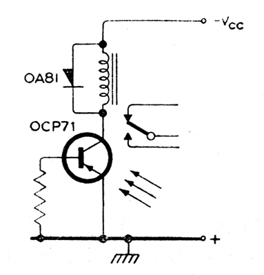
FIG. 4. Basic circuit for unmodulated light.
This circuit is adequate for on-off applications. With a base-emitter resistor of 5kΩ, the light- to dark-current ratio may be, for example, 480 at 25°C and 20 at 45°C. Without this resistor, the corresponding values may be 90 and 9.5. The resistor should preferably be an ntc type; the exact value depends on the maximum ambient temperature and the light level.
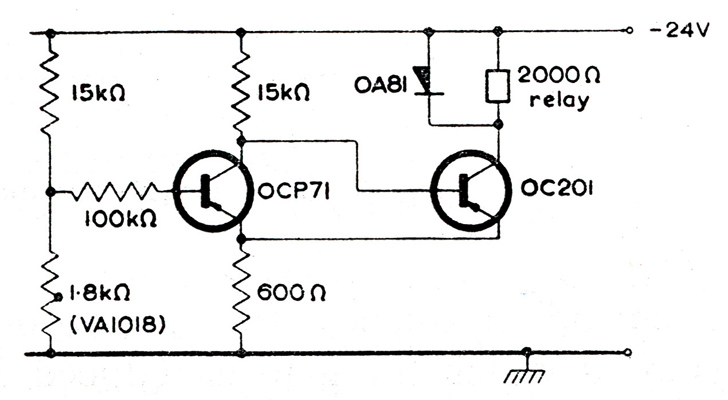
FIG. 5. Temperature compensated circuit with DC amplifier.
Fig. 5 includes an OC201, which is used as a simple DC amplifier following the OCP71 to give extra sensitivity. This circuit has temperature compensation.
Maximum dissipation in the transistor occurs at half of full drive. Maximum power is available to operate the relay when the transistor is bottomed, under full drive. For example, consider a phototransistor operating from a 20V supply. A relay of 5kΩ is in the collector. Sufficient light is available to bottom the phototransistor and 4mA flows in the collector. Thus:
Power in the load ≅ 4mA x 20V = 80mW;
Max power in the phototransistor on switching
≅ 4/2 mA x 20/2V = 20 mW;
Phototransistor dissipation when bottomed
≅ 0.15V x 4mA = 0.6 mW.
To ensure reliable operation, it may be necessary to choose a relay which will pull in at a power rather lower than four times the maximum power in the transistor.
Where temperature stability is important and a chopped light source is available, the circuit of Fig. 6 can serve as a basis for design. The base is returned to the emitter through an inductance, which is preferably parallel-tuned to the light-modulation frequency. For the modulation frequency, the base is essentially open-circuit, and maximum amplification of the light signal is obtained. For DC (dark current, or current due to unwanted background illumination), the base impedance is so low that the amplification of this current is reduced to a minimum. Stabilisation is provided by the potential divider and by the bypassed resistance in series with the emitter.
The cut-off frequency for a phototransistor is the modulation frequency at which the gain is reduced 3dB below the value with unmodulated light. The typical value is 3kHz for the OCP71 in the circuit shown in Fig. 6.
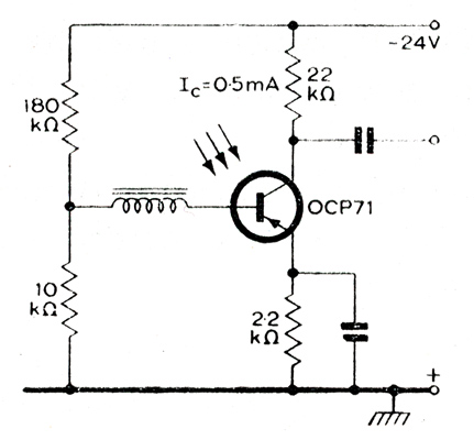
FIG. 6. Basic circuit for modulated light.
If the emitter resistor is unbypassed, AC feedback will be introduced. The overall gain will be considerably lower, but the frequency response will be considerably extended.
Applications
Special features of the OCP71 are its small size, low operating voltage, high sensitivity, relatively large sensitive area, robust construction, ability to respond to infra-red radiation, and quick response.
The OCP71 is suitable for a variety of industrial-control and other applications such as:
- Photoelectric counters
- Speed measurement
- Liquid-level controls
- Edge detection (in paper making, textiles, and belting)
- Burglar alarms
- Door opening
- Curve followers
- Smoke detection
- Industrial on/off controllers.
|